
Nano-Engineering
Professors Chang, Cohen, Christofides, Lu, Morales-Guio, Monbouquette, and Sautet
Research on surface chemistry and physics is the foundation for discovery of surface-engineered materials that have applications in the fields of separations, sensing, and semiconductors. Faculty in the Chemical & Biomolecular Engineering Department at UCLA work in the areas of macromolecular and nano-surface engineering to develop more efficient and selective membranes and sorption resins, design new molecular chemical sensors, synthesize biocompatible surfaces, and manipulate heterogeneous surface processes at the atomic scale.
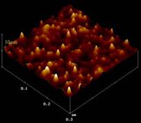
Molecular modeling and experimental investigations are geared towards understanding the structure of silylated and graft-polymerized surfaces (e.g., topology, conformation and distribution) and devising physical and chemical methods (e.g., graft polymerization and self-assembly) to control surface properties. Recent major accomplishments in this area are patented ceramic-polymer composite membranes (Cohen Group). This membrane, with a nano-structured separation layer, has proven effective in protein ultrafiltration and pervaporation separation of organic-organic and organic-aqueous mixtures.
Molecular engineering of innovative, self-assembling systems that mimic biological systems is researched to solve technological problems. For example, an approach that magnetobacteria use has been harnessed to produce the magnetite particles needed for magnetotaxis in the synthesis of semiconductor nanoparticles (Monbouquette Group). Size monodisperse, 100-nm-diameter phospholipid vesicles serve as compartments for synthesis of <10-nm-diameter II-VI semiconductor nanocrystals of tightly controlled size and composition. Size and surface-engineered particles may find applications in lasers, flat-panel displays, and quantum computing.
Professor Nobe also focuses on investigating physical properties of electrodeposited quantum dots, nanomagnets, nanowires (10 to 400 nm diam. with aspect ratios up to 18,000), nanostructured multilayers, and metal oxide and conducting polymer supercapacitors. The figure shows an example of an electrochemical nano system (ENS) where cobalt nanowires were electrodeposited from anodized alumina templates.
Molecular engineering of innovative systems that mimic biological systems is researched to solve technological problems. Since the direct manipulation of individual molecules presents obvious technological difficulties, much of the research has focused on self-assembling systems. For example, Professor Monbouquette’s group has borrowed an approach that magnetobacteria use to produce the magnetite particles needed for magnetotaxis in the synthesis of semiconductor nanoparticles. Size monodisperse, 100-nm-diameter phospholipid vesicles serve as compartments for synthesis of <10-nm-diameter II-VI semiconductor nanocrystals of tightly controlled size and composition. These nanoparticles exhibit size-dependent physical properties due to quantum confinement of electrons. Size and surface-engineered particles may find applications in lasers, flat-panel displays, and quantum computing. Monbouquette’s group is also pursuing the use of quantum dots in creating surfaces with a feature size of 2-3 nm.
Atomic layer deposition (ALD) to engineer nanometer thin films and nanolaminates with atomic resolution and controllability is also being studied (Chang Group). Highly uniform, conformal, and stoichiometric films can be easily synthesized, for example, nanolaminates can be formed through the use of multiple chemical precursors in alternating reaction sequences. ALD has been used to deposit metals, metal oxides, metal nitrides, semiconductors, transparent conductive oxides, and ferroelectric materials, with potential applications in microelectronics, membrane, sensor, bioceramic, and catalysis.


ALD Graph thin films 5ALD Graph thin films 6ALD Graph thin films
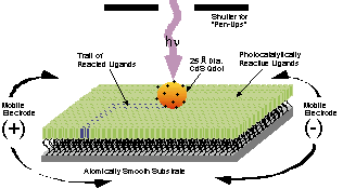
Professor Hicks’ group has developed a method of simulating reactions on compound semiconductor surfaces using molecular cluster calculations with density functional theory. Using this method, a cluster model for a gallium arsenide surface has been developed, which identified all the reaction sites on the surface as being an arsenic dimer and two second-layer gallium atoms. Each arsenic dangling bond is filled with a pair of electrons, while each gallium dangling bond is empty, in excellent agreement with experimental observations. The most exciting result from this work is the prediction of the vibrational frequencies of the optimized clusters and their excellent comparison with infrared data. This unique capability allows a definitive assignment of the observed vibrational bands to specific adsorption sites. This method is currently being applied to the study of surface reaction mechanisms for organometallic precursors.